Almost everything we encounter in our modern world relies, in some way, on electronics. Ever since we first discovered how to harness the power of electricity to generate mechanical work, we’ve created devices large and small to technologically improve our lives. From electric lighting to smartphones, every device we’ve developed consists of only a few simple components stitched together in a wide variety of configurations. In fact, for more than a century, we’ve relied on:
- a voltage source (like a battery)
- resistors
- capacitors
- inductors
These represent the core components of practically all of our devices.
Our modern electronics revolution, which relied on these four types of components plus — a little later on — the transistor, has brought us virtually every item we use today. As we race to miniaturize electronics, to monitor more and more aspects of our lives and our reality, to transmit greater amounts of data with smaller amounts of power, and to interconnect our devices to one another, we quickly run into the limits of these classical technologies. But five advances are all coming together in the early 21st century, and they’re already beginning to transform our modern world. Here’s how it’s all going down.
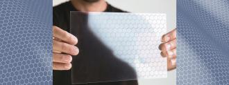
1.) The development of graphene. Of all the materials ever discovered in nature or created in the lab, diamonds aren’t the hardest ones anymore. There are six that are harder, with the hardest being graphene. Isolated by accident in the lab in 2004, graphene is a one-atom-thick sheet of carbon locked together in a hexagonal crystal pattern. Just six years after this advance, its discoverers, Andre Geim and Kostya Novoselov, were awarded the Nobel Prize in physics. Not only is it the hardest material ever, with an incredible resilience to physical, chemical, and heat stresses, but it is literally the perfect atomic lattice.
“Maybe we are on the verge of yet another miniaturization of electronics that will lead to computers becoming even more efficient in the future.”
Nobel Foundation
Graphene also has fascinating conductive properties, which means that if electronic devices, including transistors, could be made out of graphene instead of silicon, they could be smaller and faster than anything we have today. If you mixed graphene into plastics, you could transform plastic into a heat-resistant, stronger material that also conducts electricity. Additionally, graphene is approximately 98% transparent to light, meaning it has revolutionary implications for transparent touchscreens, light-emitting panels, and even solar cells. As the Nobel Foundation put it just 11 years ago, “Maybe we are on the verge of yet another miniaturization of electronics that will lead to computers becoming even more efficient in the future.”
But only if other advances also occurred alongside this development. Fortunately, they have.
2.) Surface mount resistors. This is the oldest of the “new” technologies, likely familiar to anyone who’s ever dissected a computer or cellphone. A surface mount resistor is a tiny rectangular object, usually made out of ceramic, with conductive edges on either end. The development of ceramics, which resist the flow of electric current but don’t dissipate power or heat up as much, enabled the creation of resistors that are superior to the older, traditional resistors that were used previously: axially leaded resistors.
In particular, there are enormous advantages that come along with these little resistors, including:
- small footprint on a circuit board
- high reliabilities
- low power dissipation
- low stray capacitance and inductiveness
These features make them ideal for use in modern electronic devices, particularly low-power and mobile devices. If you need a resistor, you can use one of these SMD (surface mounted devices) to either lower the size you need to devote to your resistors or increase the power that you can apply to them within the same size constraints.
3.) Supercapacitors. Capacitors are one of the oldest electronics technologies of all. They are based on a simple setup where two conducting surfaces (plates, cylinders, spherical shells, etc.) are separated from one another by a very small distance, with those two surfaces capable of holding equal and opposite charges. When you try to run current through a capacitor, it charges up; when you either turn your current off or connect the two plates, the capacitor discharges. Capacitors have a wide range of applications, including energy storage, quick bursts that release energy all at once, to piezoelectronics, in which a change in the pressure of your device creates an electronic signal.
Of course, manufacturing multiple plates separated by tiny distances on very, very small scales is not only challenging, but fundamentally limited. Recent advances in materials — in particular, calcium-copper-titanate (CCTO) — are enabling the storage of great amounts of charge in tiny volumes of space: supercapacitors. These miniaturized devices are able to charge and discharge many times before wearing out; charge and discharge much more rapidly; and store up to 100 times more energy-per-unit-volume than old-style capacitors. They are a game-changing technology, as far as miniaturized electronics go.
4.) Superinductors. The last of the “big three” to be developed, superinductors are the newest player on the scene, having only come to fruition in 2018. An inductor is basically a coil of wire, a current, and a magnetizable core all used together. Inductors oppose a change in the magnetic field inside of them, meaning that if you attempt to flow a current through one, it resists it for a time, then allows current to flow freely through it, and finally resists the change once again when you turn the current off. Along with resistors and capacitors, they’re the three basic elements to all circuits. But once again, there’s a limit to how small they can get.
The problem is that the value of inductance depends on the inductor’s surface area, which is a dream-killer as far as miniaturization goes. But rather than classical magnetic inductance, there’s also the concept of kinetic inductance: where the very inertia of the current-carrying particles themselves oppose a change in their motion. Just like ants marching in a line have to “talk” to each other in order to change their speed, these current-carrying particles, like electrons, need to exert a force on one another to accelerate or decelerate. That resistance to change creates kinetic inductance. Led by Kaustav Banerjee’s Nanoelectronics Research Lab, kinetic inductors that leverage graphene technology have now been developed: the highest inductance-density material ever created.
5.) Putting graphene in any device. Let’s take stock, now. We have graphene. We have “super” versions — miniaturized, robust, reliable, and efficient — of resistors, capacitors, and inductors. The last barrier to an ultra-miniaturized revolution in electronics, at least in theory, is the ability to transform any device, made of practically any material, into an electronic device. All we’d need in order to make this possible is to be able to embed graphene-based electronics into whatever sort of material, including flexible materials, that we desired. The fact that graphene offers good mobility, flexibility, strength, and conductivity, all while being benign to human bodies, makes it ideal for this purpose.
Over the past few years, the way graphene and graphene devices have been manufactured has come only through a small handful of processes that are themselves fairly restrictive. You can take plain old graphite and oxidize it, then dissolve it in water, and then fabricate graphene through chemical vapor deposition. However, only a few substrates can have graphene deposited on them this way. You could chemically reduce that graphene oxide, but you wind up with poor-quality graphene if you do it that way. You could also produce graphene via mechanical exfoliation, but that doesn’t allow you to control the size or thickness of the graphene you produce.
If only we could overcome this last barrier, then an electronics revolution might be close at hand.
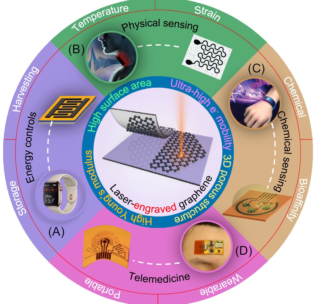
That’s where the advance of laser-engraved graphene comes in. There are two major ways that this can be accomplished. One involves starting with graphene oxide. As before: You take graphite and oxidize it, but instead of chemically reducing it, you reduce it with a laser. Unlike chemically reduced graphene oxide, this makes a high-quality product that has applications for supercapacitors, electronic circuits, and memory cards, to name a few.
You can also take polyimide — a high-temperature plastic — and pattern graphene directly onto it with lasers. The lasers break chemical bonds in the polyimide network, and the carbon atoms thermally reorganize themselves, creating thin, high-quality sheets of graphene. There have already been an enormous number of potential applications demonstrated with polyimide, since you can basically turn any shape of polyimide into a wearable electronic device if you can engrave a graphene circuit onto it. These, to name a few, include:
- strain sensing
- Covid-19 diagnostics
- sweat analysis
- electrocardiography
- electroencephalography
- and electromyography
But perhaps what’s most exciting — considering the advent, rise, and newfound ubiquity of laser-engraved graphene — lies on the horizon of what’s currently possible. With laser-engraved graphene, you could harvest and store energy: an energy-control device. One of the most egregious examples of where technology has failed to advance is the battery. Today, we pretty much store electric energy with dry-cell chemical batteries, a technology that’s centuries old. Already, prototypes of new storage devices, such as zinc-air batteries and solid-state, flexible electrochemical capacitors, have been created.
With laser-engraved graphene, not only could we potentially revolutionize the way we store energy, but also we could create wearable devices that convert mechanical energy into electrical energy: triboelectric nanogenerators. We could create superior organic photovoltaic devices, potentially revolutionizing solar power. We could create flexible biofuel cells as well; the possibilities are tremendous. On the fronts of both harvesting and storing energy, revolutions are on the short-term horizon.
Additionally, laser-engraved graphene should usher in an unprecedented era of sensors. This includes physical sensors, as physical changes, such as temperature or strain, can cause changes in the electrical properties, such as resistance and impedance (which includes contributions from capacitance and inductance as well). It also includes devices that detect changes in gas properties and humidity, as well as — when applied to the human body — physical changes in someone’s vital signs. The Star Trek inspired idea of a tricorder, for example, could quickly become obsolete by simply attaching a vital-sign-monitoring patch that alerts us to any worrisome changes in our bodies instantaneously.
This line of thought can also open up a whole new field: biosensors based on laser-engraved graphene technology. An artificial throat based in laser-engraved graphene can help monitor throat vibration, recognizing the differences in signals between coughing, humming, screaming, swallowing, and nodding motions. Laser-engraved graphene also has tremendous potential if you want to do things create an artificial bioreceptor capable of targeting specific molecules, engineer all sorts of wearable biosensors, or even help enable a variety of telemedicine applications.
It was only in 2004 that a method for producing sheets of graphene, at least intentionally, was first developed. In the 17 years since, a slew of parallel advances has finally placed the possibility of revolutionizing how humanity interacts with electronics right on the cusp of the cutting edge. Compared to all prior ways of producing and fabricating graphene-based devices, laser-engraved graphene allows simple, mass-producible, high-quality, and inexpensive graphene patterning across a wide variety of applications, including on-skin electronic devices.
In the near-term future, it wouldn’t be unreasonable to anticipate advances in the energy sector, including energy control, energy harvesting, and energy storage. Also on the near-term horizon are advances in sensors, including physical sensors, gas sensors, and even biosensors. The largest revolution will probably come in terms of wearable devices, including those used for diagnostic telemedicine applications. To be certain, many challenges and barriers still remain. But those obstacles require incremental, not revolutionary, improvements. As connected devices and the internet of things continue to take off, the demand for ultra-miniaturized electronics is greater than ever. With the recent advances in graphene technology, the future, in many ways, is already here.
This article was originally published on our sister site, Big Think. Read the original article here.